
ALTERA Quartus2 v13.1 で内蔵メモリが使えなかったので強引にフリップフロップ群で構成した

テストパターンはグラフィカルに描きたいので・・
「なんで、いまどきQuartus prime使ってないの?」というあなた、「正論です、その通りです」なんですが、シミュレーション時にテストベンチをコードで書くのが嫌だったので、テストパターンをグラフィカルに書けるUniversity Program VWFが使えるバージョンのQuartus2を使って遊んでみました。
内蔵メモリを作る
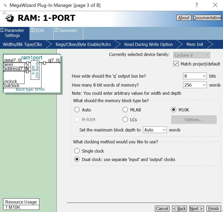
Tools ->Megawizard plug-in managerで簡単にメモリを作れます。
まあこんな感じで・・ ポチポチ押すだけの仕事です。
ところがシミュレーション時にM10Kなど作ったメモリが使えない
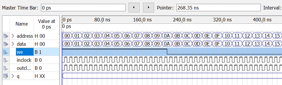
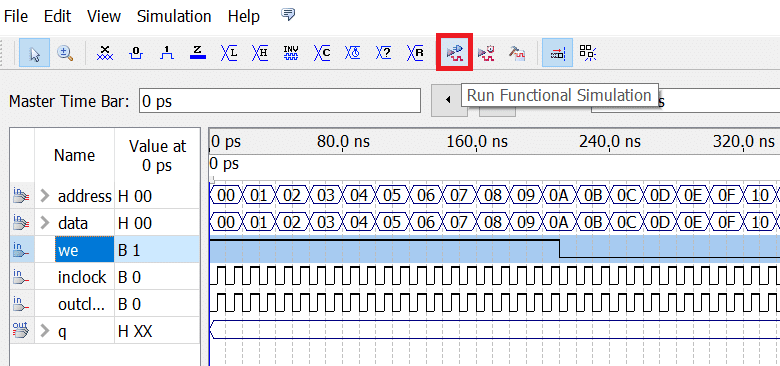
テストパターンを File -> New -> Verification/Debugging Files -> University Program WF から上図の通りグラフィカルに書きまして(1分もかからない)、下図の赤いところをポチッと押してシミュレーション開始!
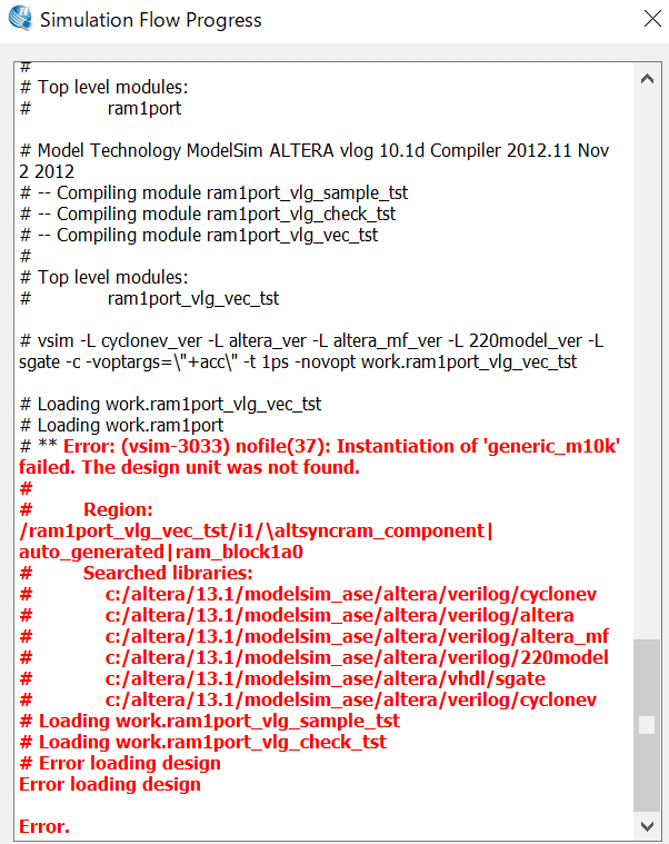
大変です 大変です 赤文字でエラーが出てます
ところがですね、数秒後にエラーがでるのでした。ライブラリがどうちゃらこうちゃら言われてますけど、VHDLで内蔵メモリ作ったからダメだったかな?? Verilogなら良さげな感じが見受けられます。が。
仕方がないので、内蔵メモリをフリップフロップ群で構成させてみる
Megawizard で吐きだした内蔵メモリ使えないじゃん、ってことでVHDLコードでメモリ相当のコードを書く。(10分程度)、ちなみにLCsと同じ動きをするメモリじゃなかったフリップフロップ群(256ワード*8bit)です。
library IEEE;
use IEEE.STD_LOGIC_1164.ALL;
use IEEE.STD_LOGIC_ARITH.ALL;
use IEEE.STD_LOGIC_UNSIGNED.ALL;

entity ff1port is
	port (	address	: in std_logic_vector(7 downto 0);
			data 	: in std_logic_vector(7 downto 0);
			we		: in std_logic;
			inclock	: in std_logic;
			outclock: in std_logic;
			q		: out std_logic_vector(7 downto 0));
end ff1port;

architecture rtl of ff1port is
	-- Define an array of 256 registers, each 8 bits wide
	type reg_array is array(255 downto 0) of std_logic_vector(7 downto 0);
	signal registers : reg_array := (others => (others => '0'));  -- Initialize all to 0

begin
	-- Writing process
	process(inclock)
	begin
		if rising_edge(inclock) then
			if we = '1' then
				registers(conv_integer(address)) <= data;
			end if;
		end if;
	end process;

	-- Reading process
	process(outclock)
	begin
		if rising_edge(outclock) then
			q <= registers(conv_integer(address));
		end if;
	end process;

end rtl;
これをそのまま論理合成するとダメなので・・
「じゃあ、このコードを論理合成してシミュレーションしてOKね」と言いたいところなんですが、この論理合成ツールが優秀なので「こいつはフリップフロップの面をかぶったメモリである、内蔵メモリとして割り当てしよっ」ってなってしまって、さっきのエラーがまた出るのでありました。
強制的に内蔵メモリとして割り当てない方法をChatGPTが教えてくれた
それでChatGPTに「強制的に内蔵メモリとして割り当てない方法」を聞いてみたところ、すぐに答えが返ってきました。「プロジェクトファイル内にある.qsfファイルに以下の1行を足し給え。」 なんだそれだけっすか。
set_global_assignment -name AUTO_RAM_RECOGNITION OFFおお、レジスタ(フリップフロップ)として割り当てられている
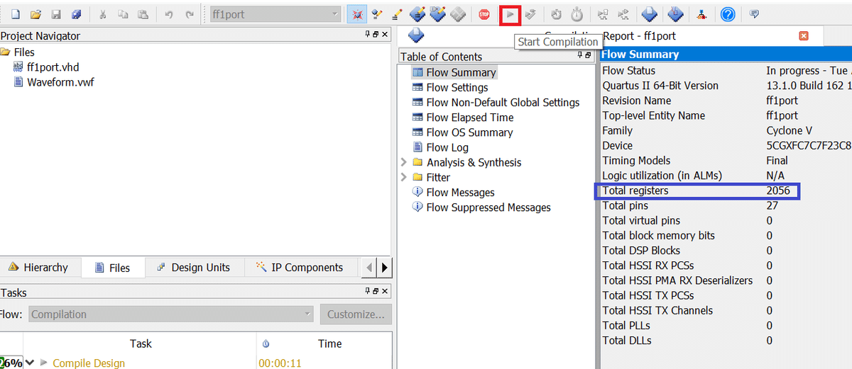
以下の論理合成中の図を見てください。(赤枠を押すとスタートする)
青枠のところがレジスタとしてアサインされたことを示していますね。
(256ワード*8+8=2056となってます)
メモリコントローラ(というかインターフェース変換)作りました
このメモリ代替フリップフロップ群はLCsの動作、インターフェースに合わせて作りましたが恐らく省エネ動作を狙った独特なインターフェースとなっているので一般的なチップセレクト、ライト、リードなどのインタフェースに合うように変換するモジュールを用意しました。と言ってもたいしたコードではないので説明するまでもないでしょう。
library IEEE;
use IEEE.STD_LOGIC_1164.ALL;
use IEEE.STD_LOGIC_ARITH.ALL;
use IEEE.STD_LOGIC_UNSIGNED.ALL;

entity mem_con2 is
    Port ( 	clk : in  STD_LOGIC;
           	reset_n : in  STD_LOGIC;
           	cs_n 	:in std_logic;
           	wr_n	:in STD_LOGIC;
           	rd_n	:in STD_LOGIC;
           	adri	:in std_logic_vector(7 downto 0);
           	wdatai	:in std_logic_vector(7 downto 0);
           	rdatai	:in std_logic_vector(7 downto 0);
           	we 		:out  STD_LOGIC;
           	adro	:out std_logic_vector(7 downto 0);
           	wdo		:out std_logic_vector(7 downto 0);
           	inclocko:out  STD_LOGIC;
           	outclocko:out  STD_LOGIC;
           	rdatao	:out std_logic_vector(7 downto 0);
           	wait_n : out std_logic);
end mem_con2;

architecture rtl of mem_con2 is
    signal istatecntw :std_logic_vector(1 downto 0);
    signal istatecntr :std_logic_vector(2 downto 0);
    signal	iwait_n1,iwait_n2	:std_logic;


begin
    process(clk, reset_n)
    begin
        if reset_n = '0' then
            istatecntw <= (others=>'0');
        elsif rising_edge(clk) then
        	if istatecntw = "10" then
        		istatecntw <= (others=>'0');
        	elsif cs_n = '0' and wr_n ='0'then
				istatecntw <= istatecntw + '1';
			elsif istatecntw /= "00" then
				istatecntw <= istatecntw + '1';
        	end if;
        end if;
    end process;


    process(istatecntw )
    begin
        if istatecntw = "10" then
			inclocko <= '1';
		else inclocko <= '0';
        end if;
    end process;

    process(istatecntw )
    begin
        if istatecntw /= "00" then
			we <= '1';
		else we<= '0';
        end if;
    end process;

    process(istatecntw )
    begin
        if istatecntw = "01" then
			iwait_n1 <= '0';
		else iwait_n1<= '1';
        end if;
    end process;

    wait_n <= iwait_n1 and iwait_n2;

    process(clk, reset_n)
    begin
        if reset_n = '0' then
            adro <= (others=>'0');
        elsif rising_edge(clk) then
        	adro <= adri;
        end if;
    end process;

    process(clk, reset_n)
    begin
        if reset_n = '0' then
            wdo <= (others=>'0');
        elsif rising_edge(clk) then
        	wdo <= wdatai;
        end if;
    end process;

    process(clk, reset_n)
    begin
        if reset_n = '0' then
            istatecntr <= (others=>'0');
        elsif rising_edge(clk) then
        	if istatecntr = "100" then
        		istatecntr <= (others=>'0');
        	elsif cs_n = '0' and rd_n ='0'then
				istatecntr <= istatecntr + '1';
			elsif istatecntr /= "000" then
				istatecntr <= istatecntr + '1';
        	end if;
        end if;
    end process;

    process(istatecntr )
    begin
        if istatecntr = "011" then
			outclocko <= '1';
		else outclocko<= '0';
        end if;
    end process;

    process(istatecntr )
    begin
        if istatecntr = "000" then
			iwait_n2 <= '1';
		else iwait_n2<= '0';
        end if;
    end process;

    process(clk, reset_n)
    begin
        if reset_n = '0' then
            rdatao <= (others=>'0');
        elsif rising_edge(clk) then
        	rdatao <= rdatai;
        end if;
    end process;

end rtl;
トップ階層でコントローラとフリップフロップ群をつなぐ
ただつなぐだけのコードです。
library IEEE;
use IEEE.STD_LOGIC_1164.ALL;
use IEEE.STD_LOGIC_ARITH.ALL;
use IEEE.STD_LOGIC_UNSIGNED.ALL;

entity mem_test2 is
    Port ( 	clk 	: in STD_LOGIC;
           	reset_n : in STD_LOGIC;
           	adr		: in std_logic_vector(7 downto 0);
           	wdata	: in STD_LOGIC_VECTOR (7 downto 0);
           	cs_n	: in STD_LOGIC;
           	wr_n	: in STD_LOGIC;
           	rd_n	: in STD_LOGIC;
           	wait_n  : out std_logic;
           	rdata	: out STD_LOGIC_VECTOR (7 downto 0);
				db_iaddress : out std_logic_vector(7 downto 0);
				db_idata	: out std_logic_vector(7 downto 0);
				db_iwe	: out std_logic;
				db_iinclocko : out std_logic;
				db_ioutclocko :out std_logic;
				db_iq :out std_logic_vector(7 downto 0));
end mem_test2;

architecture rtl of mem_test2 is
	signal iq,iaddress,idata		:std_logic_vector (7 downto 0);
	signal iwe,iinclocko ,ioutclocko		:std_logic;

	component mem_con2
    Port ( 	clk : in  STD_LOGIC;
           	reset_n : in  STD_LOGIC;
           	cs_n 	:in std_logic;
           	wr_n	:in STD_LOGIC;
           	rd_n	:in STD_LOGIC;
           	adri	:in std_logic_vector(7 downto 0);
           	wdatai	:in std_logic_vector(7 downto 0);
           	rdatai	:in std_logic_vector(7 downto 0);
           	we 		:out  STD_LOGIC;
           	adro	:out std_logic_vector(7 downto 0);
           	wdo		:out std_logic_vector(7 downto 0);
           	inclocko:out  STD_LOGIC;
           	outclocko:out  STD_LOGIC;
           	rdatao	:out std_logic_vector(7 downto 0);
           	wait_n : out std_logic);
    end component;

    component ff1port
	Port
	(
		address		: IN STD_LOGIC_VECTOR (7 DOWNTO 0) ;
		data		: IN STD_LOGIC_VECTOR (7 DOWNTO 0);
		inclock		: IN STD_LOGIC ;
		outclock	: IN STD_LOGIC ;
		we			: IN STD_LOGIC ;
		q			: OUT STD_LOGIC_VECTOR (7 DOWNTO 0)
	);
	end component;

begin

	u0:mem_con2
		port map( 	clk 	=> clk,
           			reset_n => reset_n,
           			cs_n 	=> cs_n,
           			wr_n	=> wr_n,
           			rd_n	=> rd_n,
           			adri	=> adr,
           			wdatai	=> wdata,
           			rdatai	=> iq,
           			we 		=> iwe,
           			adro	=> iaddress,
           			wdo		=> idata,
           			inclocko=> iinclocko,
           			outclocko=>ioutclocko,
           			rdatao	=> rdata,
           			wait_n => wait_n);

    u1:ff1port
    	port map(	address	=> iaddress,
					data	=> idata,
					inclock	=> iinclocko,
					outclock=>ioutclocko,
					we		=> iwe,
					q		=> iq);

	db_iaddress <= iaddress;
	db_idata	<= idata;
	db_iwe	<= iwe;
	db_iinclocko <= iinclocko;
	db_ioutclocko <= ioutclocko;
	db_iq <= iq;

end rtl;
トップ階層のプロジェクトファイル内の.qsfファイルに以下を記載する(内蔵メモリをアサインしないようにする)ことを忘れずに・・
これ重要!
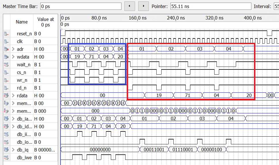
set_global_assignment -name AUTO_RAM_RECOGNITION OFF動いた!
青はライト、赤はリードですね。(データは誕生日っぽいですが私の誕生日ではありません)
どれだけの需要があるか分かりませんが、記録として残しておきたいと思います。ありがとうございました。